Article posted on Jul 8, 2019
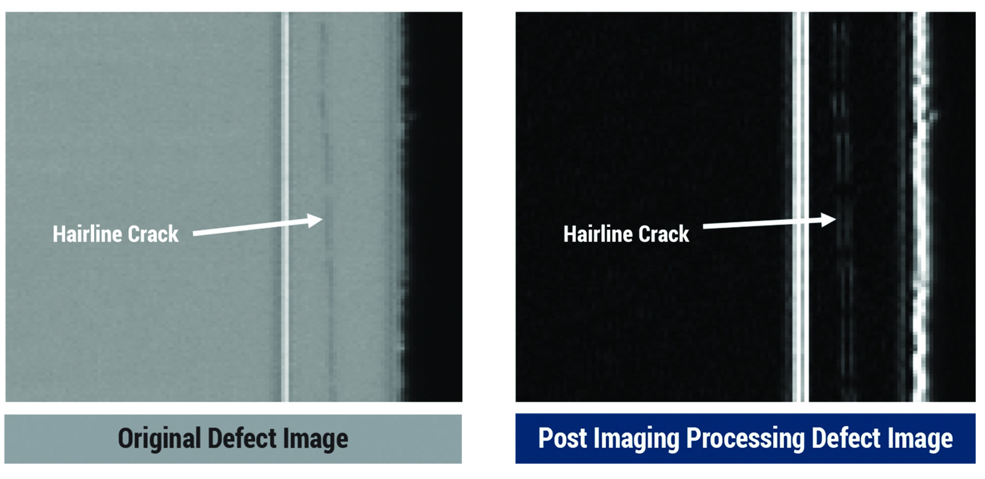
Die cracks come in several types, each requiring a different approach to optimize detection. Hairline cracks occur at the surface. They are small and shallow and show low contrast in inspection images. Sidewall cracks penetrate the die from the sidewall (the die edge), roughly in the plane of the die, and seem to be directly associated with the dicing process. Inner cracks are similar to sidewall cracks but may occur anywhere in the die and are likely caused by stresses introduced at other stages in the process. Backside cracks originate in the wafer substrate and often continue across multiple die.
As with any defect, the best approach is prevention. In the case of die cracks this requires tighter control of the dicing process. Manufacturers have relied primarily on manual inspection in this area. Like many manual processes, it is slow, labor intensive and often inconsistent. Automating the inspection process addresses these concerns.
Die cracks that may not affect yield may cause field failures and adversely impact reliability. Detecting die cracks is essential in high reliability applications, like automotive, where there are significant safety and liability concerns. Proven solutions exist for in-line crack detection in high volume manufacturing. The solution described here combines software and hardware to reduce the number of cracks that occur with improved control of the dicing process, increase the sensitivity to hairline cracks with image processing, enhance the detection of sidewall and inner cracks with IR inspection, and enable backside inspection with special handling capabilities.