Article posted on Jan 31, 2017
Fan-in wafer-level packages, such as flip chips, arrange I/O contacts over the surface of the die. The number of contacts is limited by the size of the die. Fan-out packaging processes allow chip manufacturers to increase the I/O count by artificially extending the die surface. In fan-out processes the die are embedded in an epoxy molding compound with more space between die than on the original wafer. The reconstituted substrate may mimic the shape of a wafer, allowing subsequent processing in equipment designed to handle wafers, or it may be a larger rectangular panel, conferring benefits from certain economies of scale in subsequent processing. After reconstituting the wafer/panel, the fan-out process uses thin film techniques to create redistribution layers that extend beyond the edges of the die and onto the adjacent molding compound. Finally, solder balls on contact pads atop the redistribution layer provide reliable connections to a mating printed circuit board. The additional spacing between die extends the surface area available for contacts and permits an arbitrarily large number of contacts per die.
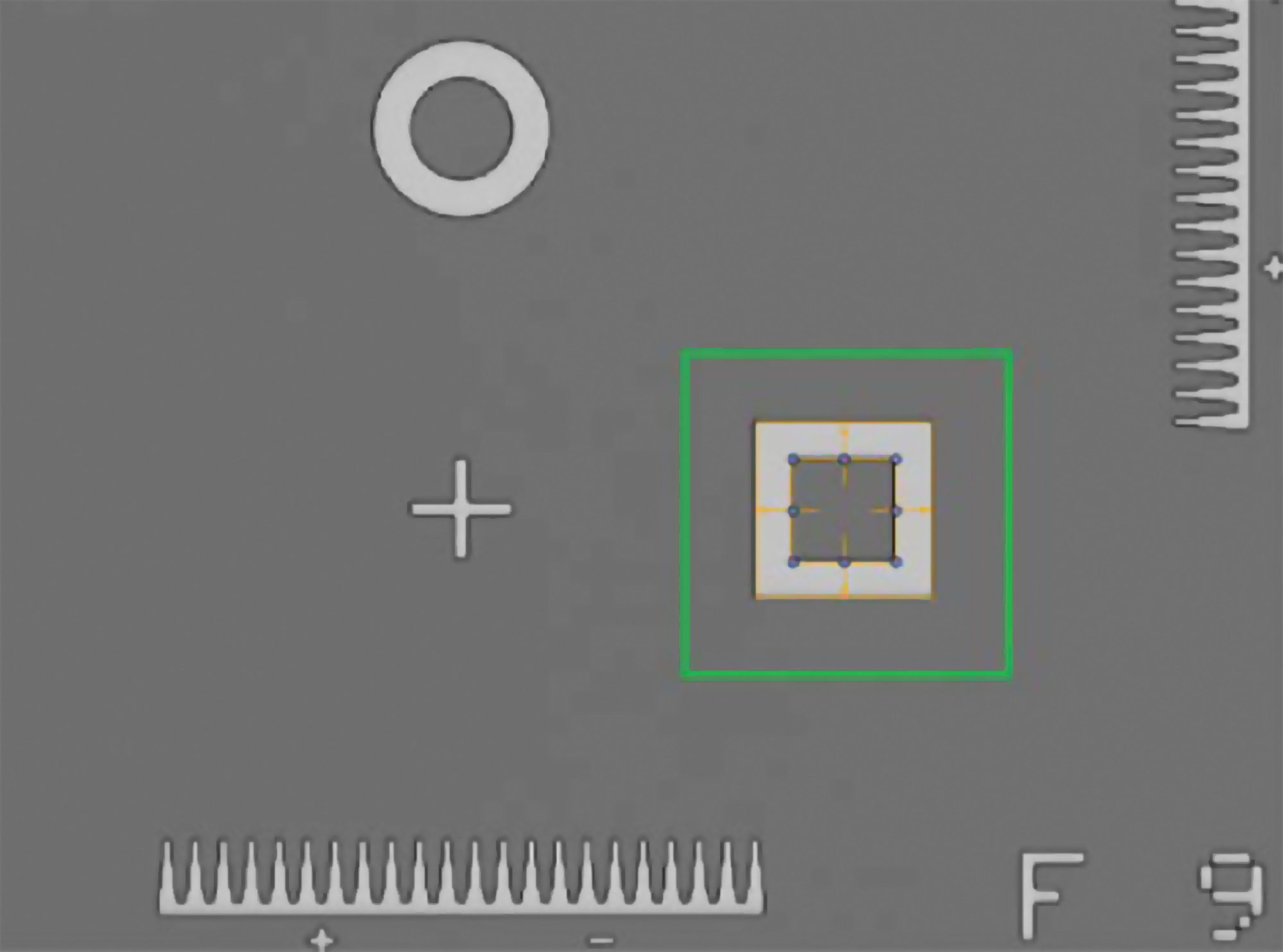
A major challenge in fan-out processing lines is the inaccuracy of die placement on the reconstituted wafer/panel. Die placement error can occur in the initial placement and during the reconstitution process, and die can also shift in subsequent processing steps. Accurate information about the location of the die is required to ensure that the interconnects formed in the redistribution layer connect with the I/O contacts of the die. Manufacturers have addressed die placement error by using a photolithography system to measure the position of each die and realign each exposure, i.e., die-by-die alignment. Although effective, the alignment process is time consuming and can amount to as much as two thirds of the overall exposure cycle.Eliminating die-by-die alignment in the exposure tool can dramatically increase its throughput, with commensurate reductions in the cost-of-ownership of lithography systems.
Here we describe an experiment designed to demonstrate efficacy of feed-forward measurements in achieving accurate overlay in an advanced packaging lithography tool (JetStep® Series, Rudolph Technologies).