Article posted on Sep 26, 2017
The semiconductor industry developed around a technology based on creating devices on round silicon wafers. In recent years, device packaging technologies for these devices have become an important consideration in allowing the industry to continue to satisfy consumer demand for increasing performance in ever shrinking space. By default, many of these packaging technologies were developed for round, silicon wafer-like substrates, however there are significant advantages to be derived from using larger, rectangular substrates, commonly referred to as panels. Panel-level packaging (PLP) brings its own set of challenges, and its optimization requires the use of equipment and materials specifically designed to meet them.
Square die do not fit well on round substrates. There is an inherent inefficiency near the wafer’s edge, where squeezing as many die as possible onto the wafer inevitably results in part of the exposure field falling uselessly in the exclusion zone, or off the wafer entirely. On a rectangular substrate, the rectangular pattern from the mask can fit perfectly, ultimately increasing the average number of die per exposure and, by extension, the throughput of the exposure process.
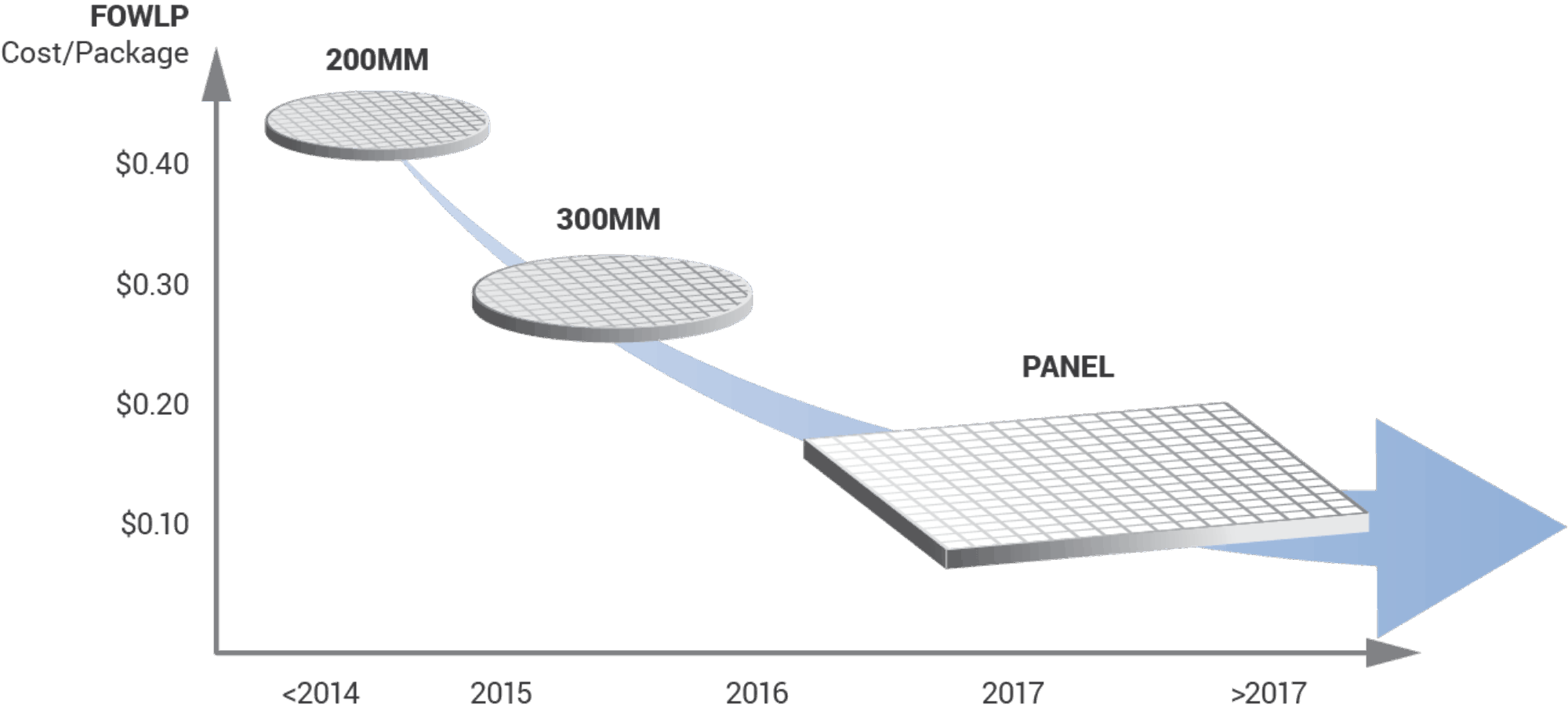
Unlike silicon wafers, panels can be produced easily at almost any size. A larger substrate increases throughput by reducing the nonproductive time spent exchanging substrates. Moreover, the same considerations that have historically driven increases in wafer size also apply to non-round, non-wafer substrates, potentially providing substantial gains from using large panels throughout the manufacturing process.
A model designed to compare 300mm round substrates with 650mm X 550mm panels [1] demonstrated significant benefits. The improved fit between die and substrate resulted in roughly 10% improvement in surface utilization. The larger size of the substrate and the improved fit between the mask and substrate reduce the transfer overhead by 5X. In this comparison, the panel-based process was estimated to reduce lithography cost per die by as much as 40%. Another study [2] estimated even greater cost reductions with further increases in panel size.
Suppliers and device manufacturers, working to develop panel-based packaging processes that take advantage of panels’ inherent benefits, face a variety of challenges, which can be grouped conveniently into two categories: equipment and materials.