Case Study posted on Jul 10, 2018
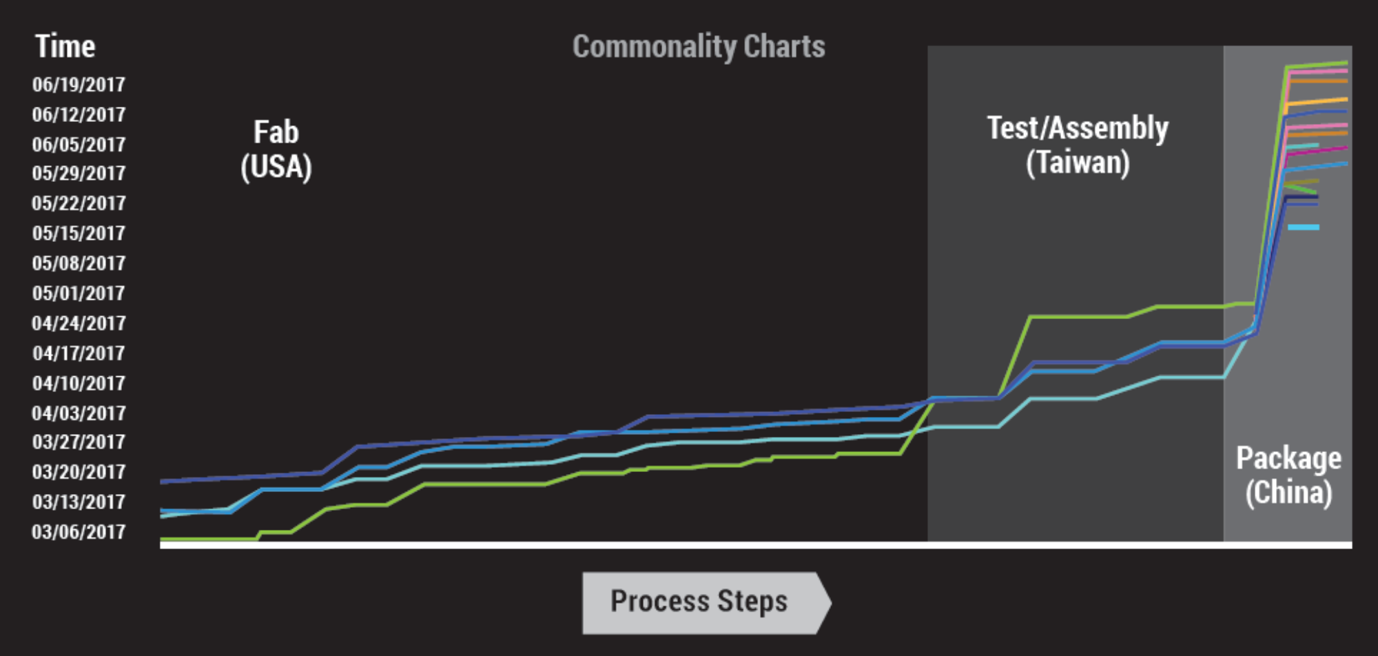
Discover Defect software collects data from the manufacturing process into a single, monolithic database that integrates vital product parameter data from every die at each step in the process with performance and condition data from all tools, factories and providers in the supply chain. It provides unprecedented visibility – sensor deep and value chain wide – of the entire manufacturing process from design, through wafer fab, test, assembly and packaging. The use of a single database means that data are available for immediate analysis rather than having first to be located and aligned from disparate databases at multiple facilities. Specialized algorithms, developed over years of experience solving yield issues and designed for big-data operations, find hidden correlations among parameters, events and conditions that can quickly guide engineers to the root causes of yield losses, ultimately delivering higher process yields and more reliable products.
This customer is a leading global supplier of electronic systems to the automotive market. Its products typically contain multiple ICs manufactured by various suppliers and facilities. Unequivocal reliability and part error rates at parts-per-billion levels is an absolute requirement because the health and safety of millions of drivers may be jeopardized by a defective product. Limiting these risks, and the associated financial liability, through fast root-cause analysis of in-house test failures, field returns and rapid identification of process drift or step function changes is a critical need. Tuning the process to improve yields while preserving critical reliability is equally important to the customer’s bottom line.
The customer is a global supplier of advanced mobile communication devices. Final modules must integrate data processing, data storage, RF communications, power management, analog sensing, and other functions, as well as contain die and components fabricated at various facilities around the world. At one point in the process, individual surface acoustic wave (SAW) and bulk acoustic wave (BAW) filters from different wafers are combined on a single substrate (panel). Figure 4 graphically shows BAW and SAW die coming together in assembly and illustrates to the user the parametric distributions of both the components and the assembled panel. and rapid identification of process drift or step function changes is a critical need. Tuning the process to improve yields while preserving critical reliability is equally important to the customer’s bottom line.