Advanced Packaging 

Whether on wafer or panel, advanced packaging offers reduced package cost and/or form factor. See how Onto Innovation can solve the most pressing challenges.

Die Shift

Real-time die shift correction

The elimination of the substrate in fan-out packaging is key to cost reduction and slim form factor. To facilitate the removal of the substrate, epoxy mold compound is used to reconstitute known good die. Both pressure and heat are used in the molding process after pick and place. In all cases, this process causes the placed die to shift and the reconstituted substrate to warp.

Onto Innovation's inspection, metrology, lithography, and advanced software are combined to dynamically measure and adjust for this shift, whether working on wafers or panels, to help ensure overlay specifications are met and subsequent RDL layers are imaged correctly.

Fine Pitch RDL

Enabling heterogeneous die integration

The need for more functionality in FOWLP and heterogeneous SiPs is driving a rapid increase in the density of redistribution layers. Line and space (L/S) widths are projected to move from the most advanced 5/5 microns to 1/1 microns and below.

With this scaling comes the need for advanced lithography and inspection to address process complexity and associated defectivity. Onto Innovation's Jetstep system offers variable NA technology and large-field imaging to allow for 1 micron L/S lithography for large form factor packages. Additionally, inspection requirements are typically 50% of the L/S specification. Onto Innovation's latest inspection systems reach below 1 micron and enable large die and package inspection to meet the challenges on current and future defect inspection requirements.

Bump metrology and analytics

Today's bumping processes create features in a wide variety of shapes, densities, quantities and materials. Collectively, they create the connections that drive device functionality, quality and yield.

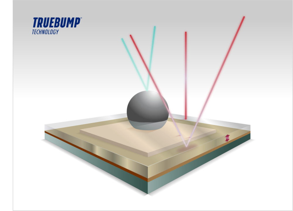
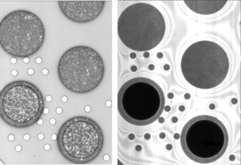
Cu pillar and microbump processes are trending toward smaller features to enable tighter integration and more functionality. The inspection and metrology required to ensure process control needs to have the resolution and accuracy to provide meaningful results that are well within the process tolerance window. Accuracy of the measurement drives all results including die-based coplanarity, average bump heights, individual bump heights and all subsequent analysis. Onto Innovation's Truebump Technology leverages multiple technologies to help ensure that thin films present on the wafer do not falsely increase or decrease the resulting bump heights being reported.

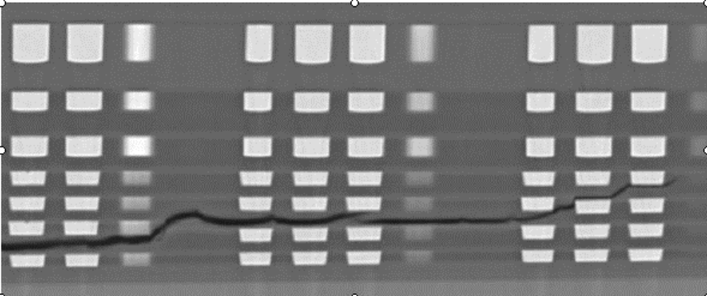
Redistribution layers and under bump metallization for smaller bumps with tighter process windows increase the complexity of the process and drive the need for more front-end like automated and sophisticated metrology systems in back-end packaging. Onto Innovation provides solutions for integrated interferometric structure step-height metrology as well as options for on-product film-stack metrology using acoustic wave technology. These 3D measurements can be augmented with high resolution 2D metrology and inspection of the same features to help ensure that RDL is meeting requirements based on design rules and that there are no process excursions leading to electrical failures.

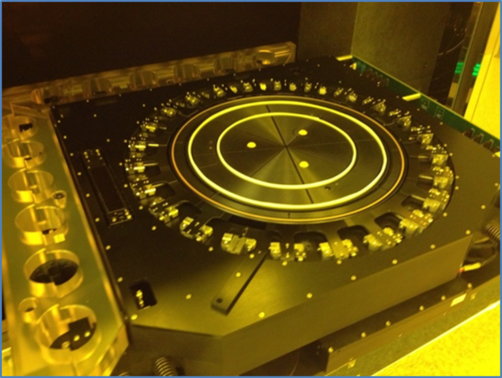
A single wafer will go through multiple process steps in the bumping process, generating layers of defect and metrology data that can be a powerful tool when handled correctly and efficiently. Onto Innovation's yield management software gives users the analytical tools to visualize data, correct process variation, and improve yield by easily analyzing multi-layer, multi-wafer and multi-lot results that include defect, 2D and 3D metrology data all in a single database with a single user interface. 

Non-Visual Defects

See previously undetected defects

Non-visual defects are a common type of process related defects in advanced packaging that stem from the lithography process which can cause degraded device performance or electrical failures. Traditional bright field and dark field inspection modes have struggled to detect these defects or provide a method to quantify their existence which has led to accepting defective devices into the downstream process.

Onto Innovation's novel approach to solve this problem provides customers a solution to detecting, controlling and fine tuning the litho process as well as helping to ensure the detection of yield-limiting defects that were previously undetectable.

Die crack detection

Detect critical reliability issues fast

Die cracks that may not affect yield may cause field failures and adversely impact reliability. Detecting die cracks is essential in high reliability applications, like automotive, where there are significant safety and liability concerns. Hairline cracks occur at the surface. They are small and shallow and show low contrast in inspection images. Sidewall cracks penetrate the die from the sidewall (the die edge), roughly in the plane of the die, and seem to be directly associated with the dicing process. Inner cracks are similar to sidewall cracks but may occur anywhere in the die and are likely caused by stresses introduced at other stages in the process. Backside cracks originate in the wafer substrate and often continue across multiple die.

As with any defect, the best approach is prevention. In the case of die cracks this requires tighter control of the dicing process. Onto Innovation combines software and hardware to reduce the number of cracks that occur with improved control of the dicing process, increase the sensitivity to hairline cracks with image processing, enhance the detection of sidewall and inner cracks with IR inspection, and enable backside inspection with special handling capabilities.

Warped Substrates

Handling adverse effects of the reconstitution process

Along with die shift issues, when pressure and heat are applied during the molding process after pick and place, a reconstituted substrate will warp. Warped substrates are uniquely challenging to handle and require specialized equipment designed to eliminate warp while being non-destructive.

Whether the process is wafer or panel based, Onto Innovation has developed handling solutions for the most warped substrates, to help ensure successful processing of the reconstituted substrate and achievement of high yields.

Consulting and Applications Services

Onto Innovation's process control consulting services allow busy manufacturers to focus on production while we examine how to improve the process.

The Onto Innovation applications teams have over twenty years of experience with hundreds of successful projects worldwide across multiple industries. Contact us today to discuss your application study needs.

Contact Us

You Have
a Challenge? We Love
a Challenge.

Let's Talk