Image Sensors 

Cameras have revolutionized the way we see the world through our mobile devices. Pixel size has decreased and the array density increased to improve camera resolution. Additionally, laser-based sensors are now being combined to integrate distance and shape recognition.

CMOS Sensor

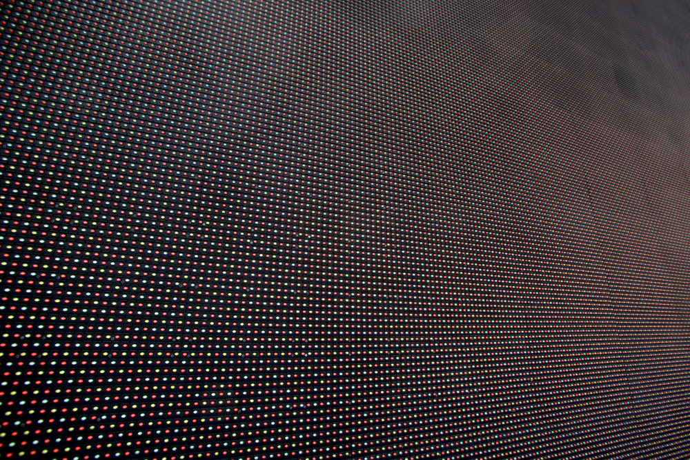
Process control of CMOS image sensor arrays

As imaging technology has improved, the challenges related to manufacturing those devices has increased. Smaller, physical pixel size, larger array areas, better quantum efficiency all present challenges for process control of this critical area. Color photo resist ADI profile, deep trench isolation etch profile and back-end metal CMP all need to be accurately controlled to enable super low noise sensing with minimal cross-talk. Additionally, the ability to find sub-micron defects as well as macro-level variations within the array is important to ensure consistent response throughout the array area.

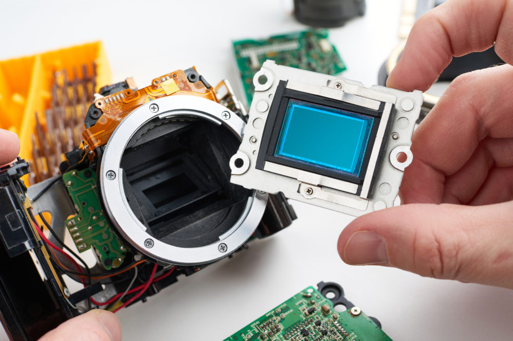
Onto Innovation enables accurate measurement and control of deep photo resist and Si channel profile/deptch for pixel isolution, as well as CMP thickness and dishing to ensure device yield. Our inspection systems control for the array area with unique image processing, creative illumination and high resolution to ensure device yield.

VCSELs

Laser-based distance and imaging 

Vertical-cavity surface-emitting lasers or VCSELs provide laser-based distance and imaging which are now combined with CMOS imagers/cameras to allow the user to see the image and identify what and where it is. To achieve this level of sophisticated 3D imaging, strict defect control, accurate metrology, and advanced data analytics are required. The combination of devices and technologies require capability to find micro-defects in the most critical regions of the device or the technology will not work correctly.

By leveraging region-specific settings on a single device and a variety of optical tools, Onto Innovation creates an adaptive inspection solution to keep up with changing technologies.

Additionally, VCSEL formation requires the deposition and etching of multiple transparent and opaque films for beam formation, wavelength, and shape. Onto Innovation provides unique ellipsometry and acoustic metrologies required to control the deposition and etch processes.

Residue

Achieve proper color response

During the colorization phase of a CMOS image sensor, the ability to find even trace amounts of residue is critical for proper color response of the imager. Onto Innovation's unique approach to detecting residual films that are not visible through traditional microscopy allows image sensor manufacturers to be confident that their process is under control. Residue detection capability is an option that can be added to a high speed defect inspection system to ensure complete utilization of the asset.

Cover Glass

Protection of the sensor

Final packaging for image sensors requires cover glass to protect the sensor and ensure long life of the device. Particles, glue residue, scratches and structural flaws in the glass all impact quality of the image even if the sensor itself is perfect. Glass substrate inspection poses certain challenges for handling and focusing. Final inspection of the image device also ensures that the attach process did not introduce foreign material residual glue that will render the device as no good.

Consulting and Applications Services

Onto Innovation's process control consulting services allow busy manufacturers to focus on production while we examine how to improve the process.

The Onto Innovation applications teams have over twenty years of experience with hundreds of successful projects worldwide across multiple industries. Contact us today to discuss your application study needs.

Contact Us

You Have
a Challenge? We Love
a Challenge.

Let's Talk