Unpatterned (Bare) Wafers and Substrates

Efficient semiconductor production and manufacturing processes start with quality control of bare silicon and epitaxial wafers. Wafer suppliers are constantly striving for improved process capability and reduced production costs by controlling critical wafer characteristics like: impurities in Si, epitaxial thickness and variation, edge and notch defect monitoring, tighter edge exclusion zones, bulk and epitaxial resistivity, and more.

Haze Detection

Detect process-related defects at full speed

The NovusEdge System utilizes background scattering (haze) data to monitor process signatures and low contrast haze defects. Haze defects can be correlated to process parameters such as surface roughness and grain size. This delivers high speed, full-wafer metrology for bare wafers and blanket films.

The capability is used for qualification and monitoring of process tools to capture blanket film defects, enabling the monitoring of defects that may be introduced during semiconductor processing steps. It is also used by IC manufacturers to ensure that incoming wafer supply meets strict quality specifications.

Elemental Contamination & EPI Thickness

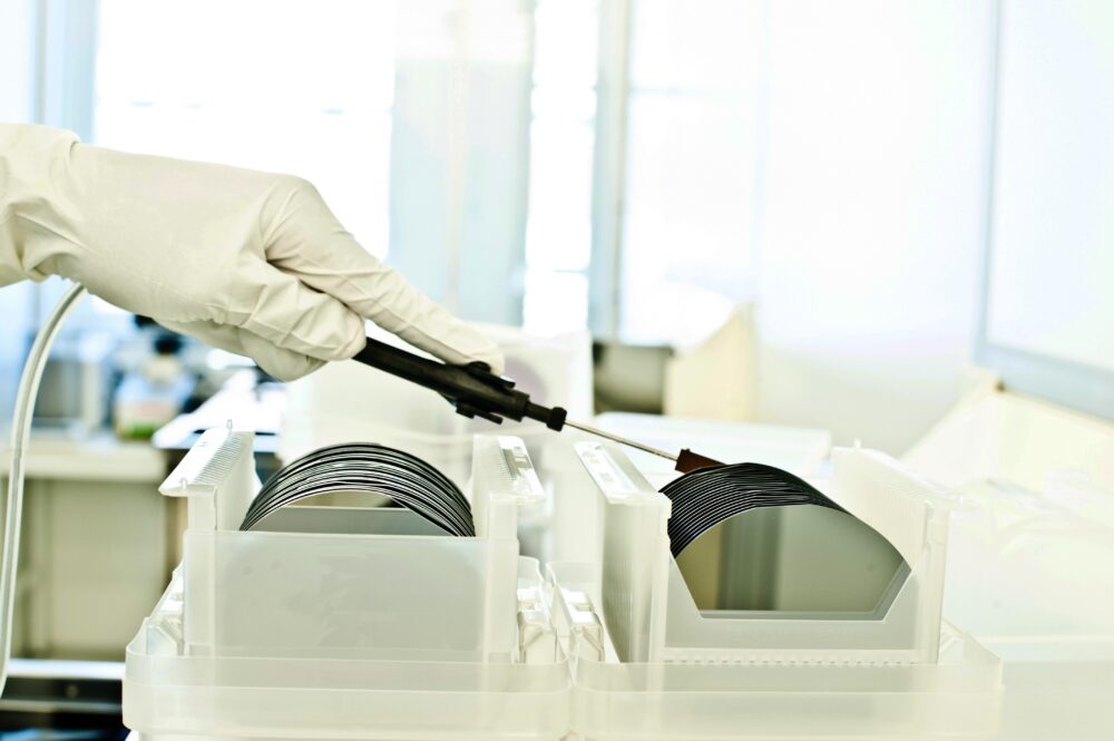
Controlling impurities in Silicon and monitoring Epi thickness and variation is the basis for improved performance of devices in the world’s electronics industry.

Measurement of Interstitial oxygen and substitutional carbon content in silicon is an important material characteristic for most modern device technologies. These measurements start at the ingot level or on thicker slugs or on thinner product wafers. Transmission based FTIR/FRS technology is used to efficiently generate oxygen profiles along the whole rod or crystal or wafers. This technique provides the wafer suppliers with rapid feedback for continuous process improvement and control. Accurate calibration to NIST certified standards and routine use of the FTIR technology has been demonstrated with minimal interference from radial oxygen gradient and predictable interference from resistivity over a wide range of product specifications.

The epitaxial layer is a thin layer of silicon typically designed to have different compositional and electrical properties from the underlying wafer, tailored to the specific demands of the device. Monitoring the thickness and the uniformity of this layer provides increased reliability during the fabrication process.

Reflection based FTIR technology is used to monitor epitaxial thickness and uniformity and provides feedback to build the most complex and sophisticated devices in the semiconductor world.

Consulting and Applications Services

Onto Innovation's process control consulting services allow busy manufacturers to focus on production while we examine how to improve the process.

The Onto Innovation applications teams have over twenty years of experience with hundreds of successful projects worldwide across multiple industries. Contact us today to discuss your application study needs.

Contact Us

You Have
a Challenge? We Love
a Challenge.

Let's Talk