A-Z Product Index
Know what you are looking for? Here's a list of all Onto Innovation products.

Know what you are looking for? Here's a list of all Onto Innovation products.

Advanced OCD metrology system for 3D NAND and high aspect ratio structures
Advanced standalone OCD & thin film metrology
Integrate equipment and factory 4.0+ systems quickly and comprehensively
The SEMI compliant foundation for optimized operations and material movement on your process equipment
Greater visibility to drive your smart factory to a cleaner operation
Your tool’s stepping stone to Industry 4.0
Revealing signals hidden in everyday noise
Your smart factory’s human classification interface
The cornerstone to factory control through recipe management
Targeting the sweet spot for your smart factory
Analytic bridge to a more profitable Industry 4.0
Automated high speed sub-micron 2D inspection and combo 3D inspection/metrology for inline process control of pattern defects and next generation technologies for advanced packaging, specialty and OQA
Edge and backside inspection
Opto-acoustic film metrology for in-line metal film thickness measurements and material characterization.
Transmission and reflection based FTIR Measurement for wafer suppliers and device makers
Advanced macro inspection for front-end manufacturers
Sub-micron automatic defect inspection for advanced IC substrates and panel level packaging
Integrated thin film and OCD metrology solution
Software solutions to increase the value of data available from your inspection tool
Metrology system for thin film and common OCD measurement
Overlay and CD metrology for the semiconductor, compound semiconductor, power devices, RF, MEMS, and LED markets
High-resolution imaging for flat panel display applications up to Gen 3.5 size
High-resolution imaging for flat panel display applications up to Gen 4.5 size
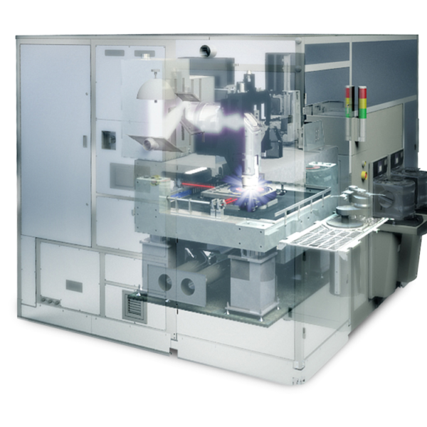
Advanced packaging lithography system for rectangular or square panel substrates up to Gen 3.5 size (720mm x 600mm)
Advanced packaging lithography system for round substrates up to 330mm
Designed for advanced integrated circuit substrates (AICS) or advanced packaging manufacturing applications, incorporating a 250mm x 250mm large field exposure area achieving 3μm L/S resolution over a large DOF and with a throughput of >110pph
Unpatterned edge, notch and backside inspection
2D automated defect inspection and sample 3D inspection for advanced packaging
Comprehensive OCD solutions for inline metrology, offline computing and fleet management
Our customers and Onto Innovation solutions: 1+1=3. Good ideas, better implementation, visionary solutions
Wafer probe card test and analysis system
The one and only automated defect classification system for smart factories
Machine learning that looks beyond known relationships