Article posted on Sep 18, 2017
Rapid growth in the mobile device market is generating demand for advanced packaging solutions with higher levels of system integration and increased I/Os and functionality. This demand is driving 2.5D/3D integration of IC devices, which in turn requires sophisticated packaging technologies. Among various approaches, fan-out is gaining traction as outsourced semiconductor assembly and test (OSAT) houses and wafer foundries roll out their own technologies. As illustrated in FIGURE 1, the adoption of fan-out technology accelerated significantly in 2016, and is projected to reach $2.5 billion by 2021, a more than 10X increase from 2015.
First generation “core” fan-out was geared toward mobile applications and had RDL lines that were typically 10/10μm (line/space) and larger. Second generation HDFO processes, which were developed to integrate multiple chips in a single package, use more RDL lines at smaller width and tighter pitch, down to 2/2μm and smaller. Growth in HDFO accelerated with the entry of Apple and TSMC in 2016 and accounts for the bulk of the fan-out growth projected through 2021.
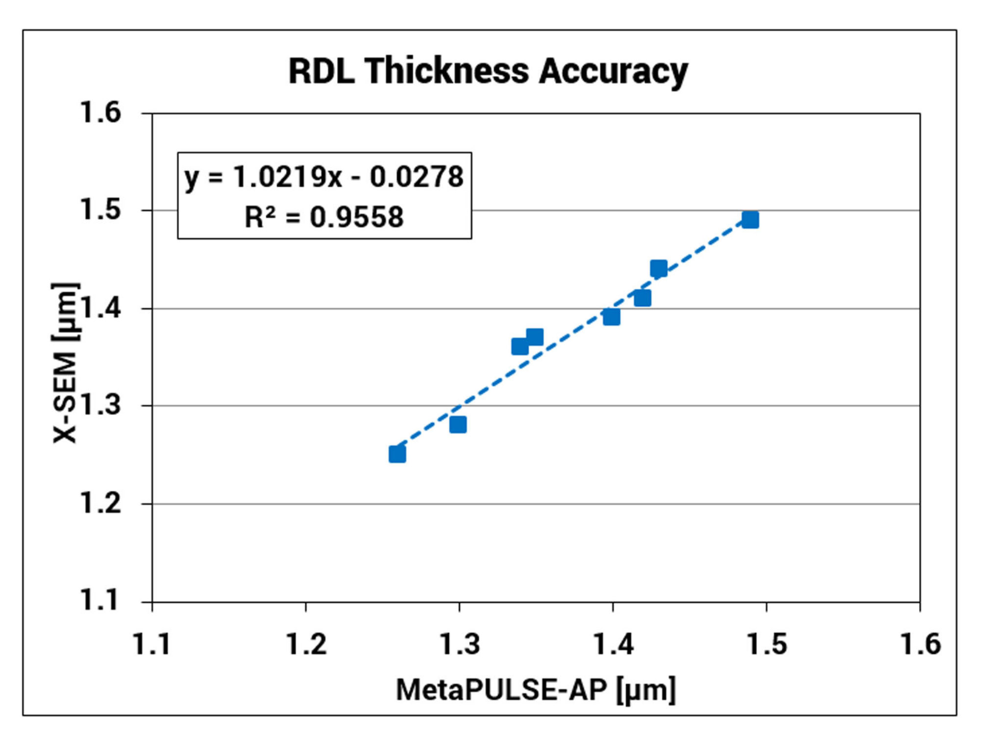
As design rules for HDFO approach those of front-end processes, so too will requirements for process control and, in consequence, the need for more accurate and repeatable metrology. Until now, manufacturers have characterized metal films, such as RDL and under bump metallization (UBM), using semi-automated measurement tools, such as contact profilometers, which are easy to use and relatively inexpensive. However, these tools are not the best solution for measuring a variety of products with varying topographies in high volume production.